
Title: Decoding the Supply Chain: Elaborating Himax's Role in 6.4T Scale-Up CPO Architecture

Disclosure: The author of this report maintains a long position in Himax. This article is for informational purposes only and does not constitute investment advice. Please see the full disclaimer at the bottom of this report.
Executive Summary
The market currently harbors a massive blind spot regarding the future of Co-Packaged Optics (CPO). While investors scramble to identify the ultimate beneficiaries of NVIDIA’s next-generation AI interconnects, the foundational hardware supply chain for TSMC’s COUPE platform is hiding in plain sight.
Himax Technologies (HIMX) represents a particularly compelling case of this market dislocation. The broader market has already recognized Foci as a primary beneficiary of the CPO revolution, bidding Foci’s market valuation up to around $2 billion. Yet, investors have entirely ignored the other half of this architectural alliance. Himax is not merely a peripheral supplier; they have serious skin in the game, holding a strategic ~5.3% equity stake in Foci. Based on Foci’s current valuation, Himax’s stake alone is now worth over $100 million. During the recent Q4 earnings call, management confirmed their direct participation in Foci’s latest equity rights issue, ensuring they maintain this highly lucrative financial foothold while helping fund the equipment purchases required for CPO mass production.
Even more telling was CEO Jordan Wu’s explicit commentary during the Q&A session regarding their “Gen 2” Wafer-Level Optics product. He confirmed that in close collaboration with an “anchor customer,” Himax and Foci are “close to finalizing the Gen 2 product, which targets bandwidth of greater than 6.4T”.
Dispelling any ambiguity about who that anchor customer might be, Wu explicitly stated that this 6.4T spec is positioned for “the AI data center market with the biggest volume potential, while demanding the highest transmission bandwidth, meaning we are talking about the GPU market”. He further quantified the potential impact of this single product line, noting that even in the early stages of mass production, it could result in “hundreds of millions of sales” for Himax.
Despite Foci’s massive inflection and these on-the-record signals from Himax’s CEO, HIMX stock has yet to reflect this fundamental shift. The broader market remains hesitant, struggling to determine whether Himax is a critical enabler of the TSMC COUPE architecture or merely a component vendor.
However, by cross-referencing three recently published patents from Himax and TSMC alongside NVIDIA’s landmark ISSCC 2026 presentation, we can build a highly compelling, evidence-based case that resolves much of this ambiguity. The technical evidence points to a highly integrated, indispensable role for the Foci/Himax alliance at the very heart of the AI data center’s most critical optical components.
Here is the technical breakdown of that integration.
The “22-Channel” Smoking Gun
To fully grasp Himax’s competitive moat, we need to examine three specific patents spanning manufacturing, metrology (testing), and foundry assembly. Across all three documents, a highly specific “22-channel” architecture repeatedly surfaces, linking the supply chain together.
1. The Manufacturing Patent (Himax)
In January 2026, Himax published a patent detailing a Nanoimprint Lithography (NIL) process for manufacturing Optical Fiber Arrays. The broader market often assumes Himax merely supplies the glass lenses. However, this patent reveals that Himax uses its NIL process to stamp both critical halves of the hardware:
The Optical Component Plate: A single, monolithic glass block stamped with 22 micro-lenses on the front, a 45-degree prism on the back, and integrated mechanical guide pins.
The V-Groove Plate: The silicon baseplate holding the microscopic trenches that the optical fibers sit in.
By stamping both the lens block and the V-groove plate, the patent suggests Himax guarantees that the channel pitch perfectly aligns, leaving Foci to act strictly as the assembler.
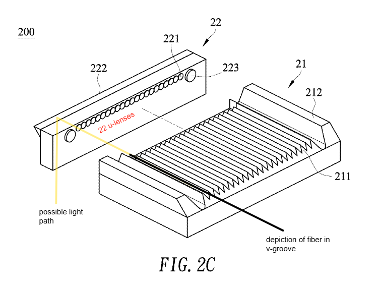
Figure 1: Himax Patent US20260003130A1 (FIG. 2C) This schematic details the architecture of the 1D linear fiber array. It illustrates the single-piece Wafer-Level Optics (WLO) block (top), which features the contiguous 45-degree prism/mirror (#222), micro-lenses (#221), and integrated guide pins (#223). This block mates vertically (top-down, rather than horizontally) against the NIL-stamped V-groove baseplate (#21). (Note: The black optical fibers and the yellow light path have been overlaid by the author to visualize the final CPO periscope mechanism. The 22 u-lenses label was also overlaid by the author).
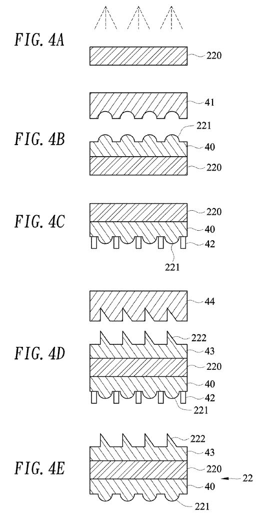
Figure 1B: Himax Patent US20260003130A1 (FIG. 4A-4E) This sequential cross-section view illustrates the specific Nanoimprint Lithography (NIL) molding steps used to form the contiguous micro-lens array (#221) and the micro-prism/mirror array (#222) on opposite surfaces of a single transparent substrate, creating the single-piece Wafer-Level Optics (WLO) periscope component.
2. The Testing Patent (Himax)
Manufacturing these microscopic blocks requires rigorous quality control. In September 2025, Himax published a patent for a highly automated 12-inch wafer-level metrology system. What exactly is this machine built to test? The patent explicitly states that it is engineered to validate contiguous glass prisms equipped with "16, 22, or 50 lenses".
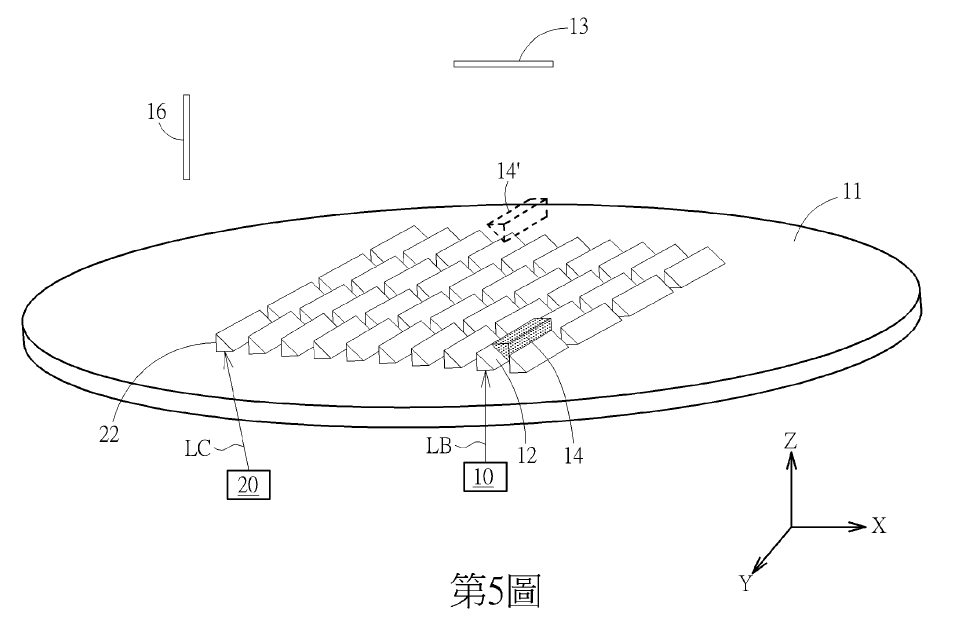
Figure 2: Taiwan Patent TWI896409B (FIG. 5) Himax’s automated wafer-level testing system. This schematic demonstrates the scale of Himax's manufacturing, showing dozens of contiguous periscope blocks on a wafer undergoing simultaneous metrology to validate optical precision. Per the text, each prism may be equipped with “16, 22, or 50 lenses” though these are not included in this schematic.
3. The Foundry Validation (TSMC)
This is where the entire supply chain aligns. Before TSMC permanently bonds an optical engine to a premium GPU, they must rigorously inspect the incoming components. In December 2025, TSMC published a patent for a Fiber Array Unit (FAU) Inspection Tool.
Look closely at the TSMC schematic from this patent:
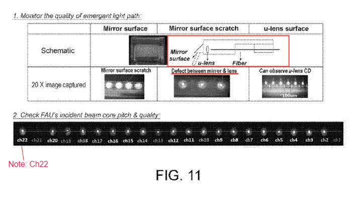
Figure 3: TSMC Patent US20250383260A1 (FIG. 11) TSMC’s metrology equipment explicitly validating a Fiber Array Unit (FAU). (Annotations added by author). The red box highlights TSMC's internal schematic of the part being tested—an exact match to the Himax contiguous WLO block sitting on a V-groove baseplate. The underlined text is the definitive proof: TSMC's cameras are inspecting for "defects between mirror & lens". This confirms they are testing a single, contiguous optical block, as defects would otherwise be located in the adhesive of separately glued parts. Finally, the bottom array explicitly confirms this is exactly a 22-channel array (Ch22).
TSMC’s equipment is actively testing an FAU with exactly 22 channels. Even more critically, look at the cross-section diagram in that exact same TSMC image. TSMC states their tool is designed to find “defects between mirror & lens”.
If the mirror (prism) and the micro-lens were separate, discrete pieces assembled by Foci, there would be no measurable solid medium "between" them—only air or a microscopic layer of optical adhesive. In that scenario, any defect would simply be a bubble in the glue. Because TSMC’s metrology cameras are specifically engineered to inspect the physical space inside the component between the mirror surface and the lens, it proves the part they are attaching is a single, contiguous block where that intervening space is a solid, continuous material. While TSMC does not name their supplier, they effectively drew the exact geometric blueprint of the Himax contiguous component—and its mating V-groove baseplate—into their own metrology patent.
How This Fits NVIDIA’s ISSCC 2026 Reveal (and the 6.4T Target)
At ISSCC 2026, NVIDIA revealed the underlying architecture for their Dense Wavelength Division Multiplexing (DWDM) CPO links. A critical detail hidden within their die photos is the deployment of vertical Grating Couplers. Because the GPU compute die is surrounded by towering High Bandwidth Memory (HBM) modules, lateral space is severely restricted. To escape the silicon, the light must shoot straight up and immediately execute a 90-degree turn to clear the memory stacks.
This physical constraint is precisely what the Himax Wafer-Level Optics (WLO) block solves. Acting as a microscopic optical periscope, the block sits directly over the grating couplers. The contiguous 45-degree prism catches the vertical light and reflects it 90 degrees horizontally, focusing it perfectly through the NIL-stamped micro-lenses and into Foci’s waiting fiber array.
But how does a 1D, 22-lens block translate to the massive 6.4T bandwidth target teased by the Himax CEO?
It all comes down to NVIDIA’s DWDM scaling math:
The Speed Upgrade: NVIDIA’s roadmap scales their DWDM microring modulators to 40 Gbps per wavelength.
The Fiber Density: With 8 data wavelengths packed into a single fiber, each individual fiber carries a massive 320 Gbps (40 Gbps × 8).
The Data Core: To achieve a 6.4 Tbps aggregate capacity, the optical engine requires exactly 20 data fibers (6,400 Gbps ÷ 320 Gbps = 20).
The Power Source: CPO engines cannot place heat-sensitive lasers directly on the hot GPU die; they require dedicated fibers to pipe in raw, continuous-wave light from an External Laser Source (ELS). Assuming standard architectures utilize 2 ELS input fibers, adding these to the 20 data fibers brings the total physical count to exactly 22 fibers—perfectly matching the Himax and TSMC patent diagrams.
The Bottom Line
The math and the mechanics perfectly align. NVIDIA’s Grating Coupler architecture strongly suggests the need for a 90-degree contiguous optical-block periscope to clear the HBM footprint. Himax holds the Nanoimprint Lithography patents to mass-produce not just that exact 22-lens glass block, but its matching V-groove baseplate. Foci brings the proprietary expertise to clamp those 22 fibers into the chassis, and TSMC has patented the exact metrology equipment required to validate this 22-channel assembly before bonding it to the chip.
The broader market is currently pricing Himax as if their role in the CPO revolution is a mere question mark. The patent trail, however, reveals them to be a highly probable cornerstone of the entire architecture.
IMPORTANT LEGAL DISCLAIMER AND DISCLOSURE
1. Ownership and Conflict of Interest The author of this report currently holds a long position in the equity of Himax Technologies (HIMX). The author may buy additional shares, sell existing shares, or close the position at any time, for any reason, without notice. The author has no business relationship with Himax, Foci, TSMC, NVIDIA, or any other company mentioned, and has not received compensation to write this report. This report is independent research and not a paid promotion.
2. Nature of “Forensic” Analysis & Basis of Opinion This report is based on a “forensic” analysis of public data, including patent filings, earnings transcripts, and technical conference papers (e.g., ISSCC). Please Note:
Inferences vs. Facts: References to “confirmation,” “validation,” “proof,” “lock,” or “smoking gun” within this report represent the author’s opinion and logical deductions based on available circumstantial technical evidence. They do not represent official confirmations or press releases from Himax, Foci, TSMC, or NVIDIA.
Speculative Connections: The connections drawn between specific patents (e.g., Himax’s Nanoimprint Lithography and TSMC’s metrology equipment) and commercial products (e.g., NVIDIA’s DWDM optical engines or TSMC’s COUPE platform) are speculative. While the author believes these connections are accurate based on the physical data presented, there is no guarantee that the companies cited are contractually or operationally linked in the exact manner described.
3. Forward-Looking Statements This report contains forward-looking statements regarding future market developments, technology adoption (e.g., Co-Packaged Optics, DWDM, and Wafer-Level Optics), and company performance. These statements are based on current expectations and assumptions that are subject to risks and uncertainties. Actual results could differ materially from those predicted due to:
Technological shifts (e.g., a move away from Grating Couplers, or alternative solutions to high-density fiber arrays).
Supply chain changes (e.g., the qualification of a second-source supplier for WLO blocks or V-groove arrays).
Macroeconomic factors or semiconductor cycle downturns. The author assumes no obligation to update any forward-looking statements or the thesis of this report should circumstances change.
4. Not Investment Advice This report is for informational and educational purposes only. It does not constitute an offer to sell or a solicitation of an offer to buy any security. The author is not a registered investment advisor, broker-dealer, or professional financial analyst. The potential outcomes discussed are strictly theoretical.
5. Accuracy, Technical Expertise, and Use of AI Tools This report was researched and drafted with the assistance of Large Language Models (LLMs) to synthesize complex technical documents. The author is an individual investor and is not a formally trained photonics engineer, semiconductor physicist, or patent attorney. While the author has reviewed the output for accuracy, the interpretation of complex legal (patent) and technical (photonics/physics) data may contain errors. Readers should verify all technical claims against the original source documents provided.
6. High-Risk Warning (Semiconductor & Emerging Tech Volatility) Investing in semiconductor and optical networking equities involves a high degree of risk and volatility. The thesis presented here relies on the persistence of specific technical barriers (e.g., Nanoimprint Lithography precision) which may be overcome by competitors or rendered obsolete by alternative architectures at any time.
YOU SHOULD CONDUCT YOUR OWN DUE DILIGENCE (DYODD) AND CONSULT WITH A QUALIFIED FINANCIAL ADVISOR BEFORE MAKING ANY INVESTMENT DECISIONS.
Sources:
Himax Technologies, Inc. Q4 Earnings Call Transcript (via Himax Investor Relations website)
US Patent US20260003130A1: Optical Fiber Array and a Nanoimprint Lithography Process for Forming the Same (Published Jan 2026, Himax Technologies Limited)
Taiwan Patent TWI896409B: Fiber array testing system (Published Sep 2025, Himax Technologies Limited)
US Patent US20250383260A1: Inspection Tool for Fiber Array Unit (FAU) Quality Monitoring in the Co-Packaged Optics Application and Methods for Inspecting Using the Same (Published Dec 2025, Taiwan Semiconductor Manufacturing Company - TSMC)