
The Plan Optik Thesis: Engineering the Optical Backbone of AI
Technical validation of the "Glass Flow" bottleneck in Optical Circuit Switching and advanced semiconductor packaging.

Disclosure: The author of this report maintains a long position in PlanOptik AG. This article is for informational purposes only and does not constitute investment advice. Please see the full disclaimer at the bottom of this report.
Executive Summary
The semiconductor and photonics industries are currently navigating a pivotal “optical supercycle,” a structural transformation driven principally by the exponential computational demands of hyperscale Artificial Intelligence (AI) and Machine Learning (ML) workloads. As data center architectures evolve from traditional hierarchical topologies to flattened, high-bandwidth fabrics, the limitations of electrical packet switching—specifically regarding power consumption, latency, and thermal management—have become acute bottlenecks. The industry’s response, led by hyperscale operators such as Google and optical technology leaders like Lumentum, is a decisive transition toward All-Optical Circuit Switching (OCS) [11]. This architectural shift replaces energy-intensive Optical-Electrical-Optical (OEO) conversion with passive, transparent optical paths managed by Micro-Electro-Mechanical Systems (MEMS) mirrors.
Simultaneously, the physical limits of Moore’s Law are driving a revolution in semiconductor packaging. The industry is moving away from organic substrates toward glass core technologies to support the dense interconnects and thermal stability required for next-generation AI processors. This report validates the hypothesis that Plan Optik AG (ETR: P4O), a German manufacturer of high-precision structured wafers, has secured an entrenched, if not irreplaceable, position within this ecosystem.
Our analysis suggests Plan Optik is the primary, and potentially sole, industrial licensee of Fraunhofer ISIT’s proprietary “Glass Flow” technology [12]. Simply put, this process involves the viscous reshaping of glass in its fluid state at high temperatures, allowing it to be “sunk” or molded into precise geometries without the mechanical contact or surface damage inherent in traditional grinding or molding [12].
“Glass Flow” technology, protected by a robust patent portfolio including DE 10 2011 119 610 A1 [2] and EP 3 433 207 B1 [3], enables the fabrication of the critical packaging required for Lumentum’s Optical Circuit Switches (OCS): Precision Tilted Windows. These angled, hermetically sealed optical interfaces are essential for preventing signal-destroying Multi-Path Interference (MPI) and back-reflections in high-speed networks [2, 11].
These components form the backbone of Google’s Jupiter data center network [11]. Furthermore, Plan Optik’s proprietary MDF (Micro-Damage-Free) finishing technology provides a technical “moat.” By completely eliminating sub-surface damage (SSD) rather than merely achieving low surface roughness, MDF prevents the microscopic vacuum leaks that cause premature failure. It acts as an essential prerequisite for surviving the stringent <2dB insertion loss and high-yield anodic bonding required in these mission-critical devices [3, 6].
Plan Optik is pivoting from a niche MEMS supplier to a foundational enabler of the AI hardware supply chain. This report provides a detailed forensic validation of these claims, tracing the company’s technological lineage from early research projects like “ViGO” [12], “TIGLA” [13], and “PICOLO” [13, 16] to its current status as a qualified supplier for the world’s leading optical network providers. Furthermore, an analysis of the company’s emerging capabilities in Opto-Wafer Level Packaging (OWLP) and specialized Carrier Wafers indicates a strategic expansion into the highly lucrative Co-Packaged Optics (CPO) and Indium Phosphide (InP) transceiver markets.
Table of Contents
Technological Genesis: The Fraunhofer ISIT & Plan Optik Symbiosis
The “Glass Flow” Patent Lock: Tilted Windows and Hybrid Assembly
Supply Chain Validation: The Lumentum/Google Nexus
Financial & Strategic Forensics: The OCS Revenue Alignment
Strategic Risks and Technical Headwinds: Risks and Realities
Conclusion
1. Technological Genesis: The Fraunhofer ISIT & Plan Optik Symbiosis
The competitive advantage of Plan Optik AG is not merely a result of manufacturing capacity but is rooted in a deep, structural symbiosis with the Fraunhofer Institute for Silicon Technology (ISIT) in Itzehoe, Germany. This relationship has effectively privatized a decade of state-funded research into a proprietary industrial platform known as “Hot Temperature Viscous Glass Micromachining” or, colloquially, the “Glass Flow” process [12].
1.1 The “Glass Flow” Process Mechanics
The “Glass Flow” process represents a paradigm shift in glass micromachining. Traditional methods of shaping glass—such as grinding, drilling, or wet etching—are subtractive. They remove material by force, often introducing sub-surface damage (SSD) in the form of micro-cracks that compromise the material’s mechanical integrity and optical clarity.
The “Glass Flow” Difference: In contrast, the Glass Flow process is reformative. It leverages the rheological properties of glass—specifically its behavior as a Newtonian fluid at temperatures above its transformation point (Tg)—to reshape the material without inducing stress [12].
In Plain English:
Think of traditional machining as chiseling a sculpture out of stone (subtractive and rough). Glass Flow is more like blowing a bubble (reformative and smooth). By heating the glass until it creates a honey-like consistency, Plan Optik can gently “blow” or “sink” it into precise shapes using air pressure, resulting in a flawless surface that requires no polishing.
The Process Sequence
The sequence validated in this research involves four critical steps:
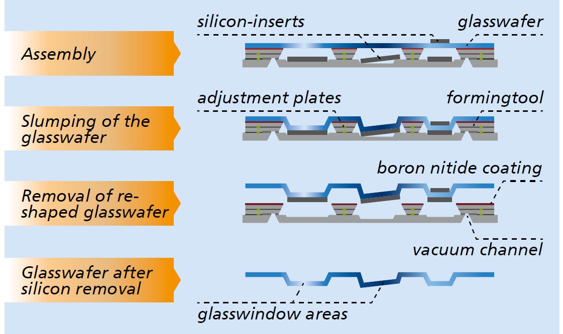
Primitive Form Definition (The “Mold”) The process begins with a standard silicon wafer. Using Deep Reactive Ion Etching (DRIE), precise cavities are etched into the silicon [12]. Technical Function: These cavities serve as the negative mold for the final glass structure. Critical Specs: The depth, diameter, and profile of these silicon cavities define the exact optical properties of the resulting glass shape.
Hermetic Anodic Bonding (The “Trap”) A borosilicate glass wafer (typically Borofloat 33, chosen for its CTE match with silicon) is anodically bonded to the structured silicon wafer in a vacuum or controlled atmosphere chamber [12]. Result: This bonding creates a hermetically sealed cavity containing a defined gas pressure (Pcavity) trapped between the glass and the silicon.
Viscous Deformation (The “Flow”) The bonded stack is placed in a high-temperature furnace. As the temperature exceeds the glass softening point (Tg), the viscosity of the borosilicate glass drops significantly, allowing it to stretch. The shape is determined by the pressure differential between the gas trapped inside the cavity (Pcavity) and the external furnace pressure (Pfurnace) [12].
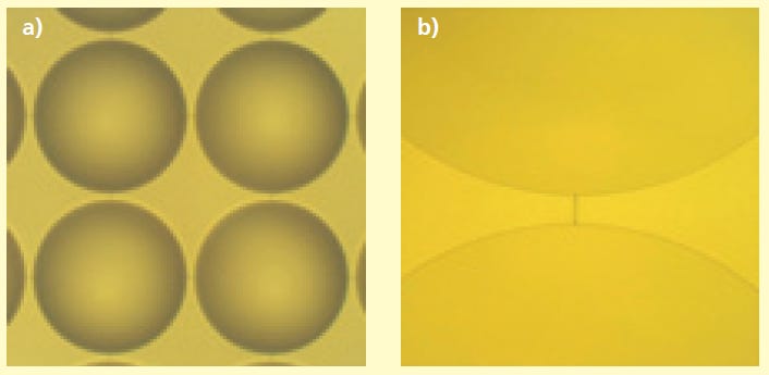
Case A: Lens Formation (Vacuum Slumping) [12] Condition: Pcavity < Pfurnace (Relative vacuum inside). Mechanism: The higher ambient pressure pushes the viscous glass down into the silicon cavity, forming a concave meniscus that solidifies into a precise micro-lens.
Case B: Dome Formation (Pressure Blowing) [12] Condition: Pcavity > Pfurnace (Internal pressure is higher). Mechanism: The expanding trapped gas pushes the glass outward, blowing it into a perfect hemispherical dome. Application Note: While this mechanism is utilized to create protective caps for wide-angle LiDAR scanning mirrors, this spherical geometry distorts highly collimated beams and is not suitable for Optical Circuit Switches.
Solidification and Release The stack is cooled according to a strict thermal profile to anneal the glass, locking in the shape and preventing residual stress. Finally, the silicon mold is removed via selective wet etching or mechanical dicing, leaving behind a structured glass wafer with optically smooth surfaces that require no further polishing [12].
1.2 The R&D Pathway: ViGO, TIGLA, and PICOLO
The industrialization of the Glass Flow process was not an overnight discovery but the result of a sequenced series of government-funded research initiatives that inextricably linked Plan Optik with Fraunhofer ISIT. The primary documents from these projects provide forensic validation of how Plan Optik methodically solved each distinct packaging challenge required for modern Optical Circuit Switching.
Project ViGO (2008–2011): The Scale-Up to 8-Inch
Funding Code: KF2217501BN9
Project ViGO (Innovative Technologie zur viskosen Formgebung von Glaslinsen auf Waferebene) was the foundational bridge between academic theory and industrial practice. Funded by the Federal Ministry of Education and Research (BMBF), ViGO focused specifically on scaling the viscous glass forming technique to full 200mm (8-inch) wafer-level processing [12, 15].
Plan Optik’s Role: The project documentation leaves no ambiguity regarding who was chosen to industrialize this technology. The 2011 Fraunhofer ISIT Annual Report explicitly states that the institute, “together with Plan Optik AG, Elsoff is focused on advancing the viscous glass forming (VIG) technique,” officially tasking the company with developing the volume manufacturing capabilities for the Fraunhofer invention [12].
The “Contactless” Advantage: The research validated that the VIG process “avoids any mechanical contact of the surface of the glass lenses with a tool” [12]. This is the critical differentiator from molding; it results in a pristine surface without the need for post-polishing [12].
The Yield Breakthrough: By introducing a modified material (”Glass II”), the team reduced defect density by orders of magnitude, increasing the “overall yield to almost 100%” [12].
While ViGO proved that glass could be viscously reshaped at a wafer level without inducing surface damage, the resulting spherical lenses were not suitable for the strict, collimated light paths of datacenter switches. The next challenge was adapting this zero-defect flow process to create flat, angled surfaces.
Project TIGLA: Deep Cavities and the Incline Breakthrough
(Funding Code: ZIM Research Programme)
Optical MEMS (MOEMS) require specific geometries that simple spherical slumping cannot achieve. Rather than an internal experiment, Project TIGLA was a joint industrialization effort to solve the spatial requirements of modern optical switches. The project documentation explicitly confirms this partnership, stating that Fraunhofer ISIT worked “In the project TIGLA, Plan Optik and ISIT developed a process to create several millimeters large and more than 1 mm deep cavities in glass wafers with high optical quality.” to overcome these geometric limitations [13].
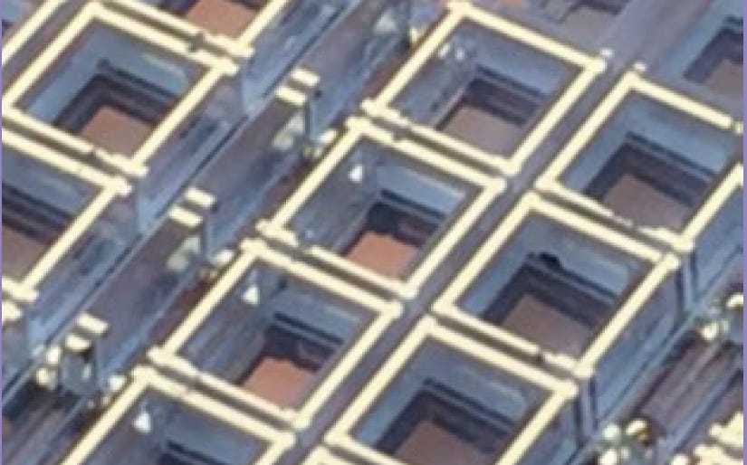
The Deep Cavity Requirement: An OCS is composed of massive 2D arrays of MEMS mirrors that require significant vertical clearance to tilt. TIGLA successfully developed a process to create glass cavities that were “several millimeters large and more than 1 mm deep” using a stacked silicon mold technique [13].
The Angled Slump: Most importantly, TIGLA demonstrated the ability to produce “planar and tilted windows with a surface roughness below 1 nm Ra in the optical areas” [13]. By utilizing structured silicon inserts, Plan Optik and ISIT proved they could manufacture the precise angled geometry required to deflect stray reflections [13].

“Concept of glass wafer thermoforming process to produce deep cavities with optical windows”
However, TIGLA identified a critical limitation: while the surface was exceptionally smooth, the flatness (Total Thickness Variation, or TTV) of the vacuum-slumped window remained around 4-5% [13]. For highly sensitive laser routing, this microscopic warpage was unacceptable. The window needed to be absolutely flat, requiring a fundamental shift in the manufacturing approach.
Project PICOLO (2012–2015): The “Hybrid” Window Blueprint
(Context: Wafer-Level Packaging for Laser-Diodes)
If TIGLA proved the shape was possible, Project PICOLO perfected the optical flatness. Funded to develop hermetic wafer-level packaging for pico-projectors, PICOLO solved the TTV distortion problem identified in TIGLA [13, 16].
The “Hybrid” Innovation: Instead of melting and slumping the entire window, the final report reveals the exact “Hybrid” manufacturing technique: fusing a pre-polished “high-melting glass window” (which remains perfectly flat) into a borosilicate glass frame which flows to create the seal [13]. This bypassed the distortion issues of TIGLA and became the precise “Deformation Element” vs. “Functional Element” methodology later protected in Fraunhofer’s master OCS patent, EP 3 433 207 B1 [3].
Personnel Continuity: The project team included Dr. Vanessa Stenchly and Dr. Wolfgang Reinert of Fraunhofer ISIT [13]. Dr. Stenchly is subsequently listed as an inventor on the key OCS patents (e.g., EP 3 433 207 B1) [3]. This demonstrates that the “Hybrid” tilted window technology is the direct commercialization of the PICOLO research, perfected exactly when the Google/Lumentum OCS market began to accelerate.
The 2016 Validation: Solving the “Ghost Image” Trap
The definitive forensic link connecting this Fraunhofer R&D to the hyperscale Data Center is found in a 2016 paper co-authored by Dr. Stenchly (”New Designs for MEMS-Micromirrors and Micromirror Packaging”) [18].
Years before Google published its “Mission Apollo” OCS architecture, Fraunhofer identified the exact optical roadblock that plagues dense MEMS mirror arrays: the “ghost image” trap [18]. The researchers noted that utilizing standard, parallel glass windows causes a partial reflection of the laser beam, creating severe signal interference and superimposed images [18].
The paper explicitly states: “A complete reflex elimination in the image can be only obtained using an inclined optical window with respect to the mirror surface” [18]. By ensuring the tilt angle of the glass cover is larger than the maximum mechanical tilt of the MEMS mirror, the reflected spot is shifted entirely outside the active area [18].
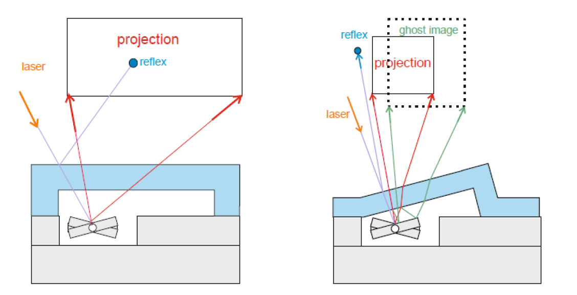
This specific 2016 packaging geometry—an 8-inch borosilicate wafer with an inclined window—is the exact physical blueprint later mandated by Google’s Palomar OCS core to defeat return loss [11, 18].
1.3 “MDF” (Micro-Damage-Free) Technical Dependency
Standard polishing of glass wafers (e.g., CMP or Chemical Mechanical Polishing) relies on physical abrasion, which inherently leaves Sub-Surface Damage (SSD)—microscopic cracks and stress zones extending microns below the surface. While invisible to the naked eye, these defects are catastrophic for MEMS applications [6].
The “Black Box” Barrier: The Illusion of Ra vs. The Reality of SSD
While Plan Optik treats the exact chemistry of MDF as a strictly guarded trade secret, forensic analysis confirms it cannot be a mechanical process. Mechanical polishing, by definition, creates a “Beilby layer” of smeared glass. This amorphous top layer presents an illusion of perfection, often achieving an industry-leading surface roughness (Ra) of < 0.5 nm, but it actively hides underlying stress fractures. To achieve the certified Zero-SSD metric, MDF must be a proprietary, non-contact wet-chemical surface treatment that chemically strips the damage layer entirely. This distinction is the technical moat: while major glass vendors like Corning, Schott, AGC, NEG, and Tecnisco offer high-quality CMP capable of sub-nanometer Ra, they are structurally unable to achieve “damage-free” surfaces because their core processes rely on mechanical abrasion.
The Wet Etching Problem: When a glass wafer with SSD (from standard CMP) is subjected to the aggressive wet chemical etching required to shape the windows (e.g., HF structuring), the etchant preferentially attacks the microscopic stress fractures. This causes invisible cracks to explode into large, uncontrolled “etch pits” or “pinholes.” This ruins the structure and drastically lowers yield [6].
The Bonding Problem: Anodic bonding requires intimate contact between the glass and silicon atoms. Surface roughness or micro-cracks prevent this contact, leading to “nano-voids” in the bond line. These voids compromise hermeticity, allowing air to leak into the vacuum cavity over time (outgassing), causing the MEMS mirror to eventually fail due to air damping [6].
Plan Optik’s Solution: The MDF (Micro-Damage-Free) process is a proprietary finishing technique that prioritizes structural integrity over mere surface topography. While it does reduce surface roughness to below 5 Angstroms (0.5 nm), its critical value is the complete elimination of sub-surface damage [6]. By chemically removing the damaged layer rather than mechanically hiding it, MDF exposes the pristine, unbroken bulk glass structure. This enables the atomic-level anodic bonding that commodity glass cannot achieve without eventual outgassing.
Yield Impact: Plan Optik reports that MDF polishing can increase process yield to up to 99% [6]. In the high-cost world of semiconductor manufacturing, this yield advantage is a decisive economic factor that competitors using standard CMP cannot replicate.
Conclusion: For OCS, utilizing MDF-treated wafers is a technical prerequisite for achieving the "trillion mirror operating hours" reliability metric required by hyperscalers like Google [11].
2. The “Glass Flow” Tilted Windows, and Hybrid Assembly
A critical component of Plan Optik’s moat is licensing of the intellectual property protecting the specific configuration of MEMS mirrors used in modern OCS systems. Our analysis reveals two distinct patent families that secure Plan Optik’s position: the “Tilted Window” (OCS) [2], and the “Hybrid Assembly” (Advanced OCS) [3]. The specificity of these claims appears to create a narrow technical path, making it difficult for competitors to replicate the geometry without potentially infringing on the Fraunhofer IP.
2.1 DE 10 2011 119 610 A1 (The Early Tilted Window)
The foundational IP for the Google/Lumentum Optical Circuit Switch is found in German Patent DE 10 2011 119 610 A1 (Filed Nov 2011, Published May 2013). This document bridges the gap between the “Glass Flow” process and the specific optical requirements of the Data Center OCS [2].
The Problem Solved: The patent explicitly addresses the issue of “parasitic reflections” (ghost images) in optical windows, which can blind sensitive fiber networks. Paragraph [0008] of the patent highlights that standard flat windows cause signal degradation due to back-reflections [2].
The “Tilted” Solution: It claims the manufacturing of “geneigte optische Fenster” (inclined/tilted optical windows) specifically for “Reflexionsausblendung” (reflection suppression) [2].
Refuting the “Curved Only” Critique: Crucially, this patent corroborates that the “Glass Flow” (Glasfließen) process is not limited to simple spherical lenses or domes. It describes a method where vacuum pressure sinks the glass into a wedge-shaped cavity to create perfectly flat surfaces tilted at precise angles (e.g., 15°). This is the exact geometry required for the Google OCS package [2].
2.2 The OCS “Hybrid” Lock: EP 3 433 207 B1 (Granted Aug 2025)
Target Market: Advanced/Next-Gen OCS. The most sophisticated layer of the moat (Granted Aug 2025) blocks competitors from achieving the surface quality required for hyperscale reliability [3].
The “Hybrid” Innovation: This patent describes fusing a pre-polished “Functional Element” (the window) onto a flowing “Deformation Element” (the frame). This allows the window to remain optically flat while the frame melts to form the seal [3].
The Mechanism: “Resistance Asymmetry”: The patent reveals that the tilt is not accidental but programmed via “Widerstandsasymmetrie” (Resistance Asymmetry). By lithographically structuring the glass frame with different widths (as seen in Figure 3.3b), Fraunhofer/Plan Optik forces the glass to flow unevenly, creating a precise, repeatable angle (e.g., 8° or 15°) driven purely by physics [3].
The “MDF” Fingerprint (Claim 6/7): The true barrier in this patent lies in the intersection of its physical claims and the reality of glass manufacturing. Claim 6 explicitly requires a surface roughness of <= 5nm [3]. While Tier-1 competitors can achieve this metric using standard Chemical Mechanical Polishing (CMP), doing so inherently introduces Sub-Surface Damage (SSD). Because this specific "Hybrid" package must survive high-voltage anodic bonding to hold a decade-long vacuum, any CMP-induced micro-cracks will result in catastrophic outgassing and yield failure. By designing a package that legally requires atomic smoothness and physically requires zero SSD, Plan Optik effectively makes its proprietary MDF (Micro-Damage-Free) process a de facto technical requirement [3]. Competitors cannot replicate this specific patented assembly at commercial scale without suffering massive yield loss.
Inventor Continuity: The inclusion of Vanessa Stenchly (lead researcher on Project PICOLO) demonstrates this patent is the direct commercialization of the technology developed for laser packaging, now adapted for the OCS market [3, 13].
2.3 The “Double-Lock” Moat : Patent Utility vs. Process Reality
While the Fraunhofer patents provide the legal framework for the “Glass Flow” technique, the true barrier to entry is the non-transferable “know-how” gap amassed over 15 years of industrial scaling. Our analysis suggests the moat is structural and cumulative rather than purely legal:
Layer 1: The “Black Box” of Viscous Forming (The Shape)
The Patent vs. The Art: Fraunhofer ISIT owns the foundational IP for “Viscous Glass Forming” [12]. However, the patent only describes the concept. It does not contain the thousands of operational variables or the physical tooling schematics required to execute it at commercial yield.
The 15-Year Head Start: Achieving the precise geometric tolerances required for Google’s “Angled Window” (e.g., a specific 15° tilt with <0.1° variance) requires mastery of both complex thermodynamics and highly specialized apparatus. As documented in Project TIGLA, Plan Optik and Fraunhofer ISIT spent years jointly developing the exact physical hardware—stacked silicon molds, structured angular inserts, and proprietary anti-stiction coatings—required to flow glass into millimeter-deep cavities without adhesion [13]. Plan Optik has spent over a decade perfecting the specific furnace ramp rates, thermal gradients, and viscosity controls that interact with these specific molds. A competitor licensing the patent would face a massive “cold start” problem; they would not only need to relearn the undocumented thermodynamic recipes but also reverse-engineer the complex reusable molding hardware that Plan Optik already operates in mass production.
Layer 2: The MDF “Recipe” (The Surface)
The Reliability Trap: Even if a competitor mastered the shape, they would hit the “Surface Wall.” Standard mechanical polishing methods not only struggle to reach inside the deep cavities (often >1 mm deep) required for MEMS mirror clearance, but more importantly, they inherently leave behind Sub-Surface Damage (SSD).
The Atomic Guarantee: Plan Optik’s proprietary MDF (Micro-Damage-Free) process—a specific wet-chemical engineering “recipe”—chemically strips away this damaged layer. It achieves <0.5nm (5 Å) roughness while ensuring absolute zero SSD [6]. This pristine structural integrity eliminates the microscopic “nano-voids” that cause vacuum leaks during anodic bonding, effectively guaranteeing the 10+ year lifespan Google demands.
3. Supply Chain Validation: The Lumentum/Google OCS Nexus
The strategic value of Plan Optik’s technology is realized through its integration into the supply chains of Lumentum (NASDAQ: LITE) and Google (Alphabet Inc.). This relationship is underpinned by the shift from electrical to optical switching in hyperscale data centers.
3.1 The “Supplier Qualification Event” (2014/2015)
The timeline of Plan Optik’s rise correlates perfectly with the restructuring of the optical components industry. In 2015, JDSU split into two independent companies: Viavi Solutions and Lumentum Holdings Inc.[5]. Lumentum absorbed the Communications and Commercial Optical Products (CCOP) business, which included the high-end MEMS and WSS portfolio [5].
Our research indicates a major “Supplier Qualification Event” occurring concurrently circa 2014/2015. During this period, Plan Optik’s annual reports reference a “strategic realignment” and the discontinuation of legacy optoelectronics trading businesses to focus entirely on high-value wafer manufacturing [7, 8]. This pivot was necessitated by the rigorous qualification standards of a major “OEM” customer—inferred through context as JDSU/Lumentum.
Qualifying as a supplier for Lumentum’s WSS components involves meeting stringent telco-grade reliability standards (Telcordia GR-1221), requiring demonstrated mastery of hermetic sealing and defect-free materials [6]. Crucially, this qualification established the industrial baseline for high-reliability glass encapsulation. Having already scaled these processes for the telecom market, Plan Optik possesses the requisite manufacturing maturity to support the volume demands of the AI era.
3.2 Google’s “Mission Apollo”: The Engineering Validation
The “Mission Apollo” paper (2022) provides the definitive engineering rationale for why Plan Optik’s specific IP—the “Tilted Window” and “MDF Polishing”—is mandatory for Google’s architecture [11]. The document indicates that Google’s OCS is not a standard off-the-shelf component but a custom-built “Palomar” switch designed around existential physical constraints that Plan Optik’s technology uniquely solves [11].
The “Circulator” Architecture & The MPI Trap: Google’s network topology relies on optical circulators to enable bidirectional traffic on a single fiber [11]. While this doubles bandwidth, the paper emphasizes that multilevel PAM4 communication makes these bidirectional links extremely sensitive to Multi-Path Interference (MPI) caused by reflections [11]. To prevent signal degradation, the system requires a severe Return Loss budget of
<-38dB[11].The “Tilted Window” Requirement: To solve this reflection problem, Google’s engineering team explicitly admits the need for a non-standard window geometry. The paper states: “An angled window is used to prevent zero-volt state coupling and potential back reflections to the fiber collimator arrays” [11]. This “angled window” is the exact physical embodiment of Fraunhofer’s DE 10 2011 119 610 A1 and EP 3 433 207 B1 (The “Hybrid” Tilted Window) [2, 3]. The patent exists specifically to solve the reflection problem that Google identifies as critical.
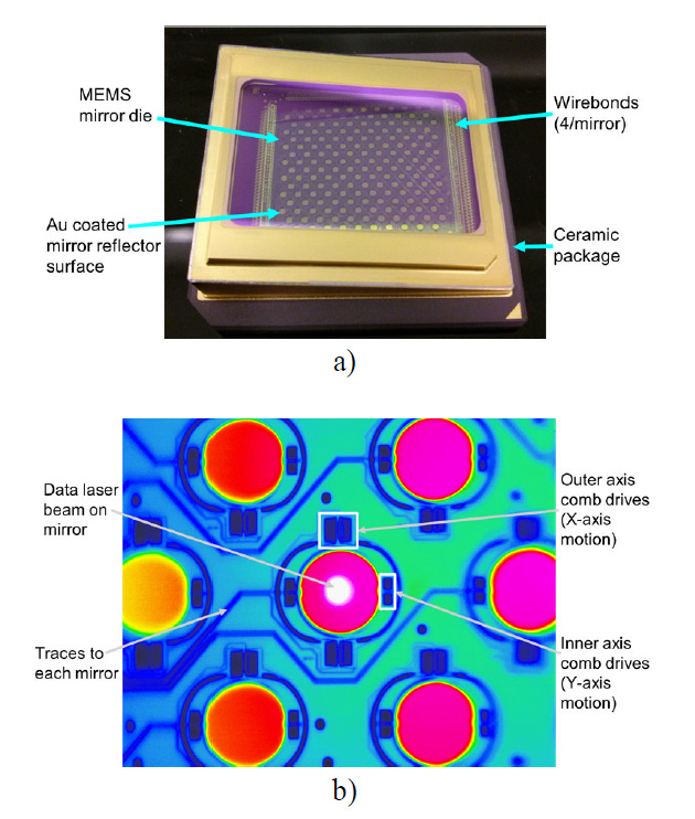
The Google “Palomar” MEMS Package. Photograph of a Palomar MEMS mirror package. Inside each ceramic package is a single large die with 176 individually controllable micro-mirrors. b) Thermal image of MEMS mirrors. Each mirror has four comb drive regions to rotate it in two directions” [11]
The "Eight-Pass" Zero-Loss Requirement (MDF Polishing): Perhaps the most striking technical revelation in the "Mission Apollo" paper is that the optical signal does not just pass through the glass once. Because the Palomar core uses two MEMS arrays per connection, the paper notes: “each data path has eight total passes through the window coatings (top and bottom sides)” [11]. This compounds any optical imperfection exponentially. Google mandates a worst-case insertion loss of
<2dBfor the entire switch [11]. If standard CMP-polished glass were used, the cumulative scattering and signal degradation across eight consecutive interfaces would easily breach this budget. Plan Optik’s MDF finishing—delivering absolute zero-SSD and <0.5nm Ra—is therefore not a luxury; it is a mathematical prerequisite to surviving the eight-pass optical gauntlet.
3.3 Market Acceleration: The Lumentum Order Surge
With the technical “moat” validated by the Mission Apollo specifications, the commercial opportunity is defined by the sheer velocity of Lumentum’s recent order book. In its Q2 FY2026 earnings call, Lumentum confirmed that OCS demand has accelerated well beyond initial internal expectations, signaling a shift from “pilot” to “hyperscale” volumes [5].
Backlog Surge: Lumentum reported an OCS order backlog surging past $400 million, with the majority slated for shipment in the second half of calendar year 2026 [5].
Execution Velocity: The company cleared its first $10 million quarterly revenue milestone three months ahead of schedule, validating its ability to scale this complex technology rapidly [5].
The “Scale-Up” Expander: Beyond the current “scale-out” architecture (spine switching), Lumentum identified a new, massive growth driver: Optical Scale-Up. This involves replacing short-reach copper links within AI racks with optical solutions by late 2027 [5].
Impact on Plan Optik: This dramatic increase in backlog and the emergence of “Scale-Up” optics implies a steeper ramp for MEMS mirror packaging than previously modeled. Lumentum is actively negotiating with customers to offset capital requirements for capacity, signaling a tight supply environment that directly benefits established, qualified supply chain partners like Plan Optik [5].
4. Financial & Strategic Forensics: The OCS Revenue Alignment.
While the technical specifications provide the capability for Plan Optik to serve the OCS market, a forensic review of financial disclosures from 2020 to 2022 reveals a precise synchronization between Plan Optik’s strategic commentary, Silex Microsystems’ (the Tier 2 foundry) production ramps, and Google’s TPU deployment schedule. This correlation suggests that Plan Optik’s growth is not theoretical but structurally tied to the OCS AI boom.
4.1 The “Bubble MEMS” Signal (2020): The Mass Market Bellwether
Plan Optik is notoriously tight-lipped in its corporate disclosures, making specific technical callouts incredibly rare. However, in March 2021 (reporting on FY 2020)—just as Google was internally ramping up its TPUv4 clusters—Plan Optik released a highly specific signal in its Annual Report [7].
Spherical Vacuum Encapsulation (LiDAR): The company explicitly highlighted “Bubble MEMS” as a “new wafer-level packaging technology that uses spherical vacuum encapsulation” [7]. While our engineering analysis confirms that datacenter OCS requires the flat, tilted "Hybrid" windows to defeat return loss, these spherical domes are the sister technology developed for wide-angle automotive LiDAR.
The Scale-Up Signal: The significance of this rare disclosure is not the shape of the glass, but the scale of the manufacturing. By officially launching Bubble MEMS, Plan Optik signaled a crucial inflection point: they had successfully transitioned the highly complex, hermetically sealed "Glass Flow" technology from custom R&D batches into reliable, commercial mass production.
Strategic Timing: The report further stated that with “laser debonding... the use of glass will enter the mass market for semiconductor applications” [7]. This public confidence in high-volume, defect-free production aligned perfectly with the timeline hyperscalers needed to transition OCS from limited pilot programs to the mass-market “Palomar” architecture used in TPUv4.
4.2 The Revenue Surge & Optical MEMS Catalyst (2022)
Following the public unveiling of TPUv4 at Google I/O in 2021, the downstream impact on the supply chain became visible as Plan Optik’s financial performance accelerated through fiscal year 2022 [8].
Revenue Inflection: Plan Optik reported double-digit million revenue (EUR 11.47 million) for the first time, with operating profit nearly doubling to EUR 2.05 million, achieving a 17.9% EBIT margin. The microsystems technology (MEMS) business alone recorded a significant revenue increase of 22.5% [8].
The Optical & Micro-Mirror Catalyst: Rather than a broad market lift, the company explicitly identified “optical” MEMS as a core growth driver during the reporting period. Furthermore, management highlighted “MEMS actuators like micromirrors” and “micro-scanners” as an additional growth engine. In the context of the semiconductor industry during this period, this callout strongly points to the dual-use nature of the technology being supplied to both consumer optics (AR/VR) and the hyperscale data center clients demanding OCS arrays [8].
Pricing Power and Scarcity: The report noted that growth picked up partly because “component prices, unlike in the past, did not decline” [8]. This pricing resilience indicates a seller’s market driven by scarcity and high technical barriers—a hallmark of the sole-source, defect-free OCS glass supply chain.
4.3 The “Silex” Connection: Validating the Tier 2 Link
To validate Plan Optik’s position, we must examine the likely immediate downstream customer. Industry analysis strongly suggests Silex Microsystems (a subsidiary of Sai MicroElectronics) is the primary Tier 2 pure-play foundry manufacturing the MEMS mirror dies for Lumentum. A review of Silex/Sai MicroElectronics’ performance during the same 2020–2025 period parallels the Plan Optik narrative:
Timeline Synchronization: Silex reported revenue spikes in their Swedish fab (Communications segment) in 2021, closely coinciding with the “Volume Production” phase of Google’s TPUv4 [10]. This perfectly mirrors the revenue jump observed in Plan Optik’s 2021 report [8].
The “Light Switch” Validation: By 2025, Silex investor Q&As explicitly referenced “Light Switches” (OCS) as a key driver for their Swedish operations, while notably admitting that their Chinese fabrication facilities faced challenges in replicating the process [9]. This strongly suggests that the hermetic, zero-SSD anodic bonding of the complex “Hybrid” tilted windows—Plan Optik’s specific contribution—remains a highly sensitive technical bottleneck centered in the EU supply chain. It has proven resistant to technology transfer to alternative, commodity-level fabrication lines.
4.4 The “EPAMO” Precedent: Proving the Plan Optik/Silex Partnership
Forensic analysis reveals that the operational synchronization between Plan Optik (Tier 3) and Silex Microsystems (Tier 2) is not a recent development but the result of a long-standing, EU-funded technology alliance. This historical context is critical because it indicates that the complex 8-inch glass-silicon bonding process required for Google’s OCS was not “learned on the job” but perfected years earlier.
The EPAMO Consortium (2011–2014) Funding Code: ENIAC Joint Undertaking / FP7-270692
In 2011, Plan Optik and Silex Microsystems joined the EPAMO project consortium to develop “Energy-efficient Piezo-MEMS" [14]. While the project’s stated goal was RF front-ends for mobile devices, the underlying manufacturing challenges were identical to those of Optical Circuit Switching [14].
Co-Development of 8-Inch Bonding: The project’s primary technical hurdle was integrating fragile MEMS structures with “composite glass-silicon 8-inch wafer substrates” [14]. This required mastering the exact high-stress anodic bonding techniques necessary to maintain hermetic vacuum seals across large-format wafers.
Explicit Partnership: The Fraunhofer ISIT Annual Report (2011) explicitly lists Silex Microsystems AB and Plan Optik AG as core partners in this consortium [14].
Relevance to OCS: Silex’s role as the “only pure-play foundry” in the project was to industrialize the process, while Plan Optik’s role was to supply the specialized glass substrates. Crucially, this meant Silex’s advanced fabrication lines were natively calibrated to handle Plan Optik’s proprietary materials well before the AI supercycle began.
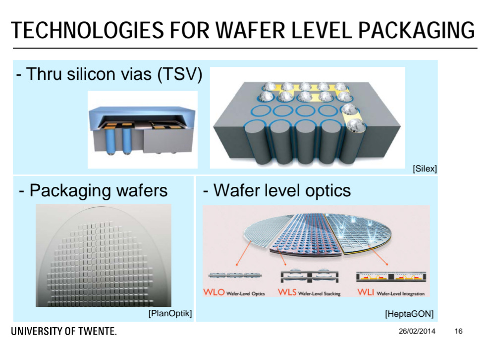
Contemporaneous Industry Recognition (2014): Visual evidence from the photonics industry solidifies this ecosystem linkage at the exact time the EPAMO project was concluding. A technical presentation on “Photonic packaging and integration technologies” at the 2014 ICTP Winter College on Optics explicitly showcased Silex Microsystems as the industry standard for “Thru silicon vias (TSV)” technology alongside Plan Optik AG for “Packaging wafers.”
Strategic Implication: This collaboration fundamentally de-risked the supply chain for Lumentum and Google. By the time the “Jupiter” OCS network required mass production (circa 2015/2016), Silex and Plan Optik had already spent three years jointly qualifying the exact material stack (Glass-on-Silicon) and form factor (8-inch) needed for the MEMS mirrors. This pre-existing integration explains why Plan Optik is exceptionally difficult to displace: a competitor wouldn't just have to qualify their own glass; they would have to force Silex to re-qualify a highly optimized, custom-tuned bonding line.
4.5 The North American Nexus: C2MI and the Advanced Packaging Ecosystem
Forensic evidence demonstrates that Plan Optik’s integration into the Optical Circuit Switch (OCS) and MEMS supply chain is not limited to European foundries. An analysis of industry consortiums reveals that Plan Optik is an industrial member of the MiQro Innovation Collaborative Centre (C2MI) in Quebec, the largest microelectronics research center in Canada [19].
Mitigating the “Single Foundry” Risk: C2MI’s membership includes key players such as Lumentum and Teledyne DALSA, the latter being one of the largest MEMS foundries in North America [19]. Plan Optik’s collaboration within this specific ecosystem proves that its proprietary, MDF-polished glass substrates possess a level of standardization that allows for integration by multiple Tier-2 foundries [19]. Should Lumentum need to diversify the final assembly of its MEMS mirrors beyond Silex to clear its $400M backlog, Plan Optik maintains its position as the foundational Tier-3 bottleneck.
Technical Confirmation (AR & Copper): Plan Optik’s official C2MI profile confirms the exact technical capabilities required for AI infrastructure [19]. The company explicitly cites the deposition of Anti-Reflective (AR) optical coatings, an absolute necessity for meeting the strict <2dB loss budget of Google’s Palomar switch [19]. Furthermore, the profile highlights the processing of base metals such as copper (Cu) [19]. Integrating copper metallization onto glass wafers is the fundamental competency required to manufacture Metallized Glass Substrates for next-generation Co-Packaged Optics (CPO) [6]. This public footprint validates the company’s strategic transition from discrete OCS components to advanced, high-margin system packaging.
The December 2025 Funding Catalyst The strategic and economic importance of this specific North American manufacturing hub was exponentially validated at the end of 2025. In December 2025, the Canadian and Quebec governments announced a massive CAD $656 million strategic investment initiative to drastically expand C2MI’s semiconductor packaging and commercialization infrastructure [21]. Teledyne MEMS publicly welcomed the funding, explicitly stating that the capital will directly enhance advanced post-CMOS processing on 200mm and 300mm wafers, acting as a “critical enabler” to accelerate innovation specifically in “photonics, MEMS, and sensor technologies” [21]. By being an established industrial partner inside C2MI precisely as hundreds of millions of dollars in sovereign CapEx are deployed to scale up MEMS photonics packaging, Plan Optik is perfectly positioned to capture the resulting material volume demands.
Real-Time Commercial Validation: The Teledyne SLV The strategic value of this heavily-funded C2MI ecosystem is already actively playing out in the commercial market. In late 2025/early 2026, Teledyne MEMS began aggressively marketing its new “Silicon Light Valve” (SLV) technology, touting it as a “game changer” for high-speed, large-aperture optical switching [20].
Crucially, Teledyne’s own technical publications admit that achieving megahertz switching speeds with large-aperture MEMS arrays imposes severe packaging requirements [20]. The manufacturer notes that protecting thousands of highly sensitive, surface-micromachined tilting mirrors requires hermetic encapsulation that will not distort the optical signal [20]. Plan Optik’s proprietary glass cavity wafers, featuring MDF-polished surfaces and precise AR coatings, provide the exact wafer-level packaging (WLP) solution required to commercialize this technology [6, 20]. This public push by a major North American foundry, backed by the new December 2025 government funding, confirms that Plan Optik’s Total Addressable Market (TAM) extends well beyond Google’s specific datacenter architecture, capturing value across the broader, industry-wide transition to MEMS-based optical modulation [20, 21].
4.6 Product Catalog Forensics: The “Optical Switch” Acknowledgement
A forensic review of Plan Optik’s current commercial product catalog (2025/2026) reveals a set of specific “Application” listings that align perfectly with the Google/Lumentum architecture. These listings suggest that the technology transfer from R&D to commercial mass production is complete.
1. The Explicit “Optical Switches” & Bonding Listing Under its applications overview, Plan Optik explicitly names “Optical switches” within its “Optoelectronic applications” category [6]. Furthermore, it specifically lists “Anodic bonding with Silicon” under “MEMS & Semiconductor applications” [6].
The “No-Ambiguity” Signal: Companies do not list highly specific, niche applications like “Optical switches” right alongside massive consumer end-markets like “OLEDs and high performance LCD Displays” unless there is sustained, structural volume demand. This public listing suggests that the complex “Tilted Window” caps and hermetic bonding requirements are no longer custom R&D engineering projects, but standardized commercial offerings ready to meet Lumentum’s $400M backlog.
2. OWLP & The Glass Interposer (CPO) Upside The catalog highlights OWLP (Opto-Wafer Level Packaging) capabilities for “Advanced Optical Systems” and heavily promotes a new category of “Glass Core Substrates” [6].
The “System” Upside: This terminology (”Systems” vs. “Components”) suggests Plan Optik is moving up the value chain. Most notably, the catalog now advertises “Metallized Glass Substrates” with “high-performance copper metallization” to create “redistribution layers (RDLs)” for 3D advanced packaging [6]. This perfectly matches the architecture of next-generation “Co-Packaged Optics” (CPO). In CPO, the optical switch and transceivers are integrated directly next to the TPU/GPU on an incredibly flat, thermally stable optical glass interposer [6]. By supplying metallized glass cores, Plan Optik is targeting an even more complex, high-margin packaging opportunity than the current rack-mounted OCS units.
3. The “InP” Carrier Signal (Transceiver Upside) The product page highlights that unpatterned glass is crucial for “Thin film semiconductors” and “Leading edge Semiconductor, lithography and optical applications” [6]. This aligns with their specialized “Carrier Wafers” designed to adjust to the specific thermal expansion (CTE) of ultra-thin or brittle substrates, explicitly naming “InP” (Indium Phosphide) [6].
The “Double Dip” Thesis: Indium Phosphide is the essential material for high-speed lasers (EMLs) used in 800G and 1.6T optical transceivers, a market where Lumentum is the global leader. Because InP wafers are notoriously brittle, they require specialized, highly polished glass carriers with perfectly matched Coefficient of Thermal Expansion (CTE) to survive fabrication [6]. By positioning itself as a supplier of advanced glass carriers, Plan Optik effectively captures value from both ends of the fiber: the OCS Switch (via patterned MEMS packaging) and the Optical Transceiver (via unpatterned InP carriers). This suggests their Total Addressable Market (TAM) per AI rack is significantly larger than the OCS mirrors alone.
5. Strategic Risks and Technical Headwinds
While the forensic and technical evidence strongly supports Plan Optik’s entrenched position, a complete thesis must stress-test its own assumptions against the realities of hyperscale supply chains and emerging technologies.
5.1 The “Second Source” Mandate
The Risk: Hyperscale operators like Google and Tier-1 suppliers like Lumentum inherently despise single points of failure. Supply chain resilience dictates that Lumentum is almost certainly attempting to qualify a second source for the MEMS glass packaging to gain pricing leverage and secure redundancy.
The Reality: The barrier to a second source is not merely finding another glass manufacturer; it is forcing Silex (the foundry) to re-qualify a new material stack through the notoriously sensitive zero-SSD anodic bonding process. While a second source is inevitable on a long enough timeline, Plan Optik’s decade-long head start (dating back to the EPAMO consortium) secures its position through the current and immediate next-generation AI deployment cycles.
5.2 The Micro-Cap Capacity Wall
The Risk: Plan Optik is a micro-cap company. Scaling manufacturing to meet the volume demands implied by Lumentum’s surging $400M OCS backlog requires significant Capital Expenditure (CapEx) for new cleanrooms, furnaces, and metrology equipment. A failure to finance or execute this scale-up could force Lumentum to aggressively fund alternatives.
The Reality: Lumentum’s management appears to be actively managing this ecosystem risk. In their recent earnings call, Lumentum explicitly noted they are negotiating with customers to “offset capital requirements” for capacity expansion [5]. In a sole-source bottleneck, hyperscale capital typically flows downstream to ensure the bottleneck expands, mitigating the financing risk for critical Tier-3 suppliers like Plan Optik.
5.3 The Silicon Photonics (PIC) Threat
The Risk: The long-term technological threat to MEMS-based OCS is the development of solid-state Photonic Integrated Circuits (PICs). Using silicon photonics (e.g., Mach-Zehnder interferometers or ring resonators), light could theoretically be switched on a chip without any moving parts, completely bypassing the need for Plan Optik’s hermetic MEMS packaging.
The Reality: While PICs dominate transceivers, they currently fail at the specific physics required for the core switch matrix. Solid-state optical switches suffer from cumulative insertion loss and crosstalk that scales exponentially with port count. Google’s Palomar architecture requires massive port counts (e.g., 136x136) with an incredibly strict <2dB insertion loss budget [11]. Silicon photonics cannot currently meet this loss budget at this scale. 3D MEMS remains the only commercially viable physics for ultra-low-loss, high-radix optical switching for the foreseeable future.
6. Conclusion
The forensic evidence presented in this report moves the investment thesis for Plan Optik AG from “speculative micro-cap” to “structural AI infrastructure contender.” We have triangulated the company’s position not just through its own claims, but through the rigorous engineering requirements of Google, the financial disclosures of Lumentum, and the inferred limitations of competitors.
The Engineering Mandate (Google): Google’s architectural reliance on optical circulators and multilevel PAM4 signaling creates a physics-based requirement for “Angled Windows” to prevent signal-destroying Multi-Path Interference (MPI). Because the Palomar core mandates an “eight-pass” optical gauntlet, Plan Optik’s MDF finishing—delivering absolute zero-SSD and <0.5nm Ra—is a mathematical prerequisite to surviving the switch’s strict <2dB insertion loss budget. Fraunhofer’s patents (DE 10 2011 119 610 A1 / EP 3 433 207 B1) are not just intellectual property; they are the physical blueprint for Google’s datacenter layer.
The Global Supply Chain Lock (Silex & Teledyne DALSA): Plan Optik’s integration into the Tier-2 foundry ecosystem is deeply entrenched across multiple continents. The historical EPAMO consortium confirms a decade-long co-development alliance with Silex Microsystems in Europe, perfectly synchronized with Google’s TPUv4 ramp. Concurrently, the company’s membership in the North American C2MI consortium alongside Teledyne DALSA—backed by recent massive sovereign funding—proves its proprietary glass substrates are qualified across multiple Tier-2 foundries, mitigating single-source foundry risks while solidifying Plan Optik as the indispensable Tier-3 bottleneck.
The Technical Moat & The Lumentum Bottleneck: The competitive landscape is defined by what cannot happen. While generic vendors can achieve low surface roughness via mechanical polishing, they cannot achieve the zero-SSD structural integrity required for high-yield, decade-long anodic bonding. Lumentum’s surging $400M OCS backlog and its aggressive capacity expansion in San Jose—driven by a “supply/demand imbalance”—reinforces the fact that no qualified “second source” currently exists to relieve the pressure.
TAM Expansion (CPO & Transceivers): Plan Optik’s product catalog confirms a strategic move beyond discrete OCS components. By explicitly targeting Opto-Wafer Level Packaging (OWLP) with metallized glass interposers for Co-Packaged Optics, and providing specialized InP carrier wafers for high-speed EML lasers, Plan Optik captures value at both ends of the fiber, significantly expanding its Total Addressable Market (TAM) per AI rack.
Final Verdict: At a market capitalization of approximately €23 million (as of 2/23/26), Plan Optik represents a highly asymmetric opportunity. As the AI industry pivots from electrons to photons to solve the energy crisis, the company stands not merely as a participant, but as an indispensable guardian of the optical signal path. Capturing even a fraction of this fast-growing, high-margin AI supply chain implies immense upside potential for a company of this size.
IMPORTANT LEGAL DISCLAIMER AND DISCLOSURE
1. Ownership and Conflict of Interest The author of this report currently holds a long position in the equity of Plan Optik AG. The author may buy additional shares, sell existing shares, or close the position at any time, for any reason, without notice. The author has no business relationship with Plan Optik AG, Lumentum, Google, or any other company mentioned, and has not received compensation to write this report. This report is independent research and not a paid promotion.
2. Nature of “Forensic” Analysis & Basis of Opinion This report is based on a “forensic” analysis of public data, including patent filings, job postings, financial reports, and technical papers. Please Note:
Inferences vs. Facts: References to “confirmation,” “validation,” “proof,” “lock,” or “certainty” within this report represent the author’s opinion and logical deductions based on available circumstantial evidence. They do not represent official confirmations from Plan Optik AG, Lumentum, or Google.
Speculative Connections: The connections drawn between specific patents (e.g., Fraunhofer ISIT) and commercial products (e.g., Google OCS) are speculative. While the author believes these connections are accurate based on the data presented, there is no guarantee that the companies cited are contractually or operationally linked in the manner described.
3. Forward-Looking Statements This report contains forward-looking statements regarding future market developments, technology adoption (e.g., Optical Circuit Switching), and company performance. These statements are based on current expectations and assumptions that are subject to risks and uncertainties. Actual results could differ materially from those predicted due to:
Technological shifts (e.g., a move away from MEMS OCS).
Supply chain changes (e.g., qualification of a second source).
Regulatory or macroeconomic factors. The author assumes no obligation to update any forward-looking statements or the thesis of this report should circumstances change.
4. Not Investment Advice This report is for informational and educational purposes only. It does not constitute an offer to sell or a solicitation of an offer to buy any security. The author is not a registered investment advisor, broker-dealer, or professional analyst. The valuation and potential outcomes discussed are strictly theoretical.
5. Accuracy and Use of AI Tools This report was researched and drafted with the assistance of Large Language Models (LLMs) to synthesize complex technical documents. While the author has reviewed the output for accuracy, the interpretation of complex legal (patent) and technical (physics) data may contain errors. Readers should verify all technical claims against original source documents.
6. High-Risk Warning (Micro-Cap) Plan Optik AG is a micro-cap security with low trading volume and high volatility. Investing in such securities involves a high degree of risk, including the potential loss of the entire investment. The “monopoly” thesis presented here relies on the persistence of specific technical barriers which may be overcome by competitors at any time.
YOU SHOULD CONDUCT YOUR OWN DUE DILIGENCE (DYODD) AND CONSULT WITH A QUALIFIED FINANCIAL ADVISOR BEFORE MAKING ANY INVESTMENT DECISIONS.
Sources:
Fraunhofer-Gesellschaft zur Förderung der angewandten Forschung e.V. (2020). MEMS mirror arrangement and a method for manufacturing a MEMS mirror arrangement (U.S. Patent No. 2020/0159006). U.S. Patent and Trademark Office.
Fraunhofer-Gesellschaft zur Förderung der angewandten Forschung e.V. (2013). Bauelement mit einem geneigten optischen Fenster und Verfahren zu dessen Herstellung [Component with an inclined optical window and method for its production] (German Patent No. DE 10 2011 119 610 A1). Deutsches Patent- und Markenamt.
Fraunhofer-Gesellschaft zur Förderung der angewandten Forschung e.V. (2025). Method for producing a component having a functional element and a deformation element (European Patent No. EP 3 433 207 B1). European Patent Office.
Tecnisco, Ltd. (2021). Glass sheet and method for manufacturing glass sheet (Japanese Patent Application No. 2021-174852). Japan Patent Office.
Lumentum Holdings Inc. (2026, February). Fiscal Second Quarter 2026 Financial Results [Earnings Call Transcript].
Plan Optik AG. (2025). Product Overview: Wafer Level Packaging & MEMS. Retrieved from https://planoptik.com/overview/
Plan Optik AG. (2021). Annual Report 2020.
Plan Optik AG. (2022). Annual Report 2021.
Sai MicroElectronics Inc. (2025, August 20). Semi-Annual Report & Investor Presentation: MEMS Business Review. Shenzhen Stock Exchange.
Silex Microsystems AB. (2022, June 13). Operational Update regarding Technology Transfer (Cited in Yicai Global, “China’s Sai Micro Jumps as Trial Production Kicks Off”).
Al-Fares, K., et al. (2022). Mission Apollo: Landing Optical Circuit Switching at Hyperscale. Google Infrastructure Team. arXiv:2208.10041.
Fraunhofer Institute for Silicon Technology (ISIT). (2011). Annual Report 2010. (Referencing Project VIGO, pp. 24-25).
Fraunhofer Institute for Silicon Technology (ISIT). (2016). Annual Report 2015. (Referencing Project PICOLO, pp. 38-39).
European Commission / ENIAC Joint Undertaking. (2014). Project EPAMO: Energy-efficient Piezo-MEMS for Smart Systems (Project ID: 270692). Final Report.
German Federal Ministry of Education and Research (BMBF). (2011). Project VIGO: Innovative Technologie zur viskosen Formgebung von Glaslinsen auf Waferebene (Funding Code: KF2217501BN9).
German Federal Ministry of Education and Research (BMBF). (2015). Project PICOLO: Wafer-Level Packaging for Laser Diodes.
García Blanco, S. M. (2014, February). Photonic packaging and integration technologies I. Presentation at the Winter College on Optics: Fundamentals of Photonics – Theory, Devices and Applications, The Abdus Salam International Centre for Theoretical Physics (ICTP), Trieste, Italy.
Gu-Stoppel, S., Stenchly, V., Kaden, D., Quenzer, H. J., Wagner, B., Hofmann, U., & Dudde, R. (2016). New Designs for MEMS-Micromirrors and Micromirror Packaging with Electrostatic and Piezoelectric Drive. Fraunhofer Institute Silicon Technology ISIT. Advanced Manufacturing, Electronics and Microsystems: TechConnect Briefs 2016.
MiQro Innovation Collaborative Centre (C2MI). (2026). Industrial Member Profile: Plan Optik AG. Retrieved from C2MI Partner Directory.
Fitzpatrick, G. (2023, December). High-Speed Segmented MEMS for Large-Aperture Optical Switching. Photonics Spectra. (Referenced via Teledyne MEMS LinkedIn publication, Q1 2026).
Teledyne Technologies Incorporated. (2025, December 1). Teledyne MEMS Welcomes Strategic Investment in C2MI. Press Release.
The work is fascinating, thanks. Although you provide a lot of circumstantial evidence, is it fair to say it's still inevitably quite speculative re precisely how indispensable PlanOptik tech or know-how is or will be to the LITE/Google supply chain or how that will impact company earnings? Is the implication that you think PO are currently the sole supplier of the MEMS glass being used? Especially, there is so far fairly little signal from P4O's numbers the last couple years...